
Anjali Sharma
GG News Bureau
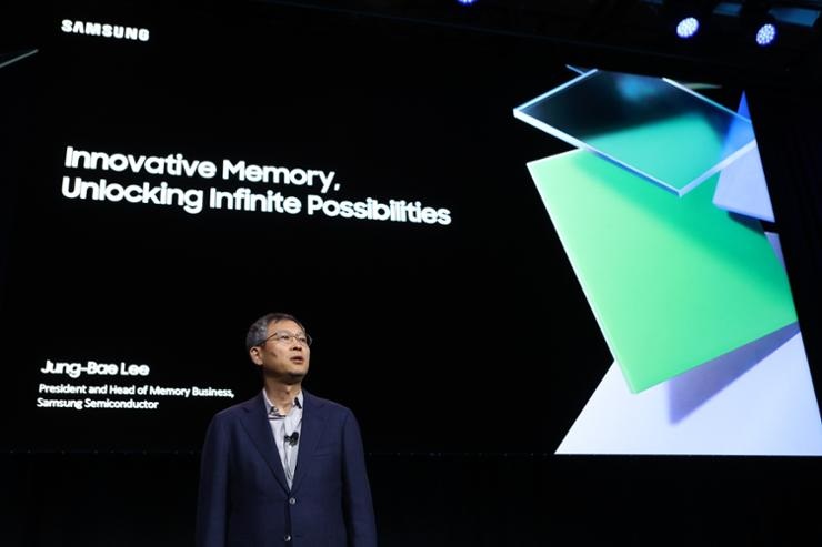
NEW YORK, 30th Jan. Samsung the world’s biggest memory chip maker on Monday has created a new research lab in the US to focus on developing next-generation three-dimensional (3D) DRAM, industry sources said on Sunday.
According to sources the company succeeded in commercializing 3D vertical NAND flash memory chips for the first time in the industry in 2013.
The new lab is operating under Device Solutions America headquartered in Silicon Valley, which oversees Samsung’s semiconductor production in the US, and will work to develop an upgraded DRAM model to allow Samsung to lead the global 3D memory chip market, the sources said.
Samsung said it is preparing new 3D structures for sub-10-nanometer DRAM, allowing larger single-chip capacities that can exceed 100 gigabits, reports Yonhap news agency.
The global semiconductor industry’s revenue declined 8.8 per cent in 2023 due to a slowdown in enterprise and consumer spending.
According to Counterpoint Research the AI provided positive news to the semiconductor industry, emerging as a key content and revenue driver, especially in the second half of the year.
Samsung was affected by the memory market slowdown in both DRAM and NAND segments, reported a 38 per cent YoY decline in its revenue.
The memory market was hit by soft demand in the PC, server and smartphone segments as well as oversupply and excess inventory across the market.